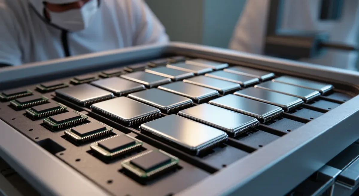
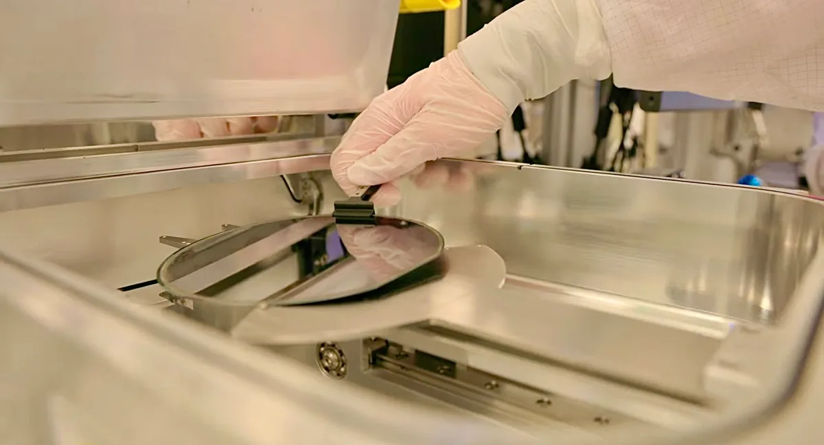
A semiconductor wafer is a thin slice of crystalline silicon that serves as the base for building integrated circuits. Chips are printed onto it in a grid, then cut apart and packaged. The price of the chips you buy depends less on the wafer itself and more on a single number: how many of those printed chips actually work.
That number is the yield. A fab pays roughly the same to process a wafer whether 90 percent of its chips pass testing or 40 percent do. The working chips alone carry the entire cost of the disc, so yield curves quietly decide who can sell memory, processors, and sensors at a profit — and who cannot.
What exactly is a wafer?
A wafer is a thin, round slice of semiconductor material, almost always silicon, used as the substrate for microelectronic devices. According to Wikipedia's entry on wafers in electronics, the term appeared in the 1950s to describe thin round slices of germanium or silicon, and the discs now serve both chip fabrication and, in square form, solar cell manufacturing.
The round shape is not decorative. It comes from the way the material is made: a seed crystal is pulled from a bath of molten silicon, growing a cylinder called a boule. The boule is sliced with a wire saw, etched to remove sawing damage, and polished until the surface is flat to within a fraction of a nanometer. The same source documents the purity involved — 99.9999999 percent, often called nine-nines, or higher. At that level, only a handful of stray atoms are allowed per billion silicon atoms. For related coverage, see NTIA's $21 Billion BEAD True-Up Rewrites America's Broadband Building Plans.
Wafers come in standard diameters that define entire generations of factories. A fab is named for the disc it is tooled to run: 200 mm fabs are the older, smaller class, while the current state of the art is the 300 mm wafer, about 12 inches across. Larger discs mean more chips per processing run, which is why the industry keeps pushing diameter upward. A 450 mm wafer has been made experimentally, but per the same reference it is not in general use.
How does a wafer become thousands of chips?
Turning a blank disc into working chips is a repeating cycle of printing, altering, and peeling away material. The core steps run in a loop hundreds of times:
- Pattern. Light projects a circuit design onto a light-sensitive coating, tracing one layer of the chip in miniature.
- Etch. Chemicals remove material everywhere the pattern exposes, carving the layer into shapes.
- Dope and deposit. Ions are implanted to change the silicon's electrical behavior, and thin films of metal or insulator are laid down.
- Repeat. A modern chip needs dozens of such layers, each aligned to the ones below with nanometer precision.
When the stack is complete, a diamond-edged saw dices the wafer into individual chips, called dies. Each die is then packaged — mounted in a protective case with connections to the outside world. Everything before dicing happens to the whole wafer at once, which is why bigger wafers changed the economics: a 300 mm disc carries roughly 640 dies of 100 mm² each, versus 269 on a 200 mm wafer, per the size table in the Wikipedia reference.
What is yield, and why is it so hard?
Yield is the fraction of dies on a wafer that pass final testing. It is never 100 percent, and the reason is physics, not sloppiness. Every step in the loop can go wrong: a particle lands where it should not, an etch cuts too deep, an alignment drifts by a few atoms. Any single fatal defect kills that die.
Defects cluster. A scratch across one region of the disc destroys every die it crosses, while the rest of the wafer is untouched. This is where die size matters more than most buyers realize. A large chip — a big GPU or a server processor — offers a huge target. One defect is more likely to land on it, and the wafer holds fewer of them to begin with, so each loss is a bigger share of the total. Small dies tolerate defects far better simply because there are more chances per disc.
Yield also improves over a product's life. Early production runs of a new design run at low yields while engineers trace the failure patterns back to specific process steps. Fixes land, yields climb, and the cost per good chip falls. That ramp is one of the most closely guarded numbers in the industry, because it is effectively the price floor.
How does yield decide who wins on price?
The arithmetic is unforgiving. If a processed wafer costs the same regardless of outcome, then cost per good die equals wafer cost divided by working dies. Double the yield, halve the cost. A competitor with a steeper learning curve can sell the same chip for less and still make margin, because more of each expensive disc turns into sellable product.
What this means for buyers: yield differences explain price gaps that specs alone never do. Two chips with identical feature lists can carry very different price tags if one was made on a mature, high-yield process and the other on a fresh one. It also explains why memory makers selling into tight markets have pricing power — when demand absorbs everything a fab can produce, low-yield early production still finds buyers, and the pressure to discount disappears. This connects to our earlier piece, Samsung, SK Hynix and Micron Have Reportedly Sold Out 2027 Memory Capacity.
Yield economics also shape strategy beyond pricing. Companies design around it. Some split large chips into smaller pieces connected together, because several medium dies with one bad piece beat one giant die with a single fatal flaw. Others deliberately disable part of a working die to sell it as a cheaper product tier — recovering revenue from a disc that would otherwise be scrapped. None of this shows up on a spec sheet, yet all of it traces back to how many dies survived the wafer.
Why wafer sizes keep growing
The push from 200 mm to 300 mm wafers, completed across the industry in the 1990s, shows the logic plainly. Per the Wikipedia size table, a 200 mm disc yields 269 dies of 100 mm²; a 300 mm disc yields 640 of the same dies — well over twice the output for one pass through the fab. Each wafer, whatever its size, takes a similar number of process steps, so the bigger disc spreads fixed effort across more salable chips.
The catch is capital. Tooling a fab for a new wafer diameter means rebuilding nearly everything, and the equipment must hold larger discs to even tighter tolerances. The 450 mm effort stalled for exactly that reason: the research was real, but the hurdles — per the same source, serious ones — never cleared to the point of general adoption. Bigger is better only when the machines to handle it can be built and paid for.
The same tension plays out at the material level. Wafers for high-power and radio-frequency devices use different growth methods than standard logic chips, trading volume for material quality. Silicon carbide wafers for electric-vehicle power electronics run smaller and cost more per die, which is one reason those chips carry premium prices even as silicon costs fall.
The takeaway: yield is the hidden price tag
Every chip price a consumer sees — in a phone, a car, a laptop — has a wafer's yield curve buried inside it. The disc itself is a commodity of astonishing purity, polished to atomic flatness and sliced into hundreds of identical chances. What separates a profitable chip line from a money-losing one is how many of those chances survive the hundreds of process steps between blank silicon and packaged part.
That is also why chip industry news so often turns on manufacturing details rather than product announcements. When a new process node ramps, when a fab is tooled for a different wafer size, or when demand lets early low-yield production sell at full price, the effects land in retail prices months later. Yield is invisible on the box. It is rarely invisible on the invoice.