Graphene is a material one atom thick — a single sheet of carbon atoms — whose isolation in 2004 earned Andre Geim and Konstantin Novoselov the 2010 Nobel Prize in Physics. Two decades on, the question is whether it can be manufactured at scale and price. In late 2025 the evidence finally pointed both ways.
What is graphene, and why did it excite everyone?
Carbon atoms bonded in a flat hexagonal lattice form a sheet with an unusual combination of properties: it is exceptionally strong yet flexible, conducts electricity and heat efficiently, and is nearly transparent despite being a single layer. Because it is fundamentally a surface — every atom is on the outside — graphene's behavior is dominated by its edges and faces, which is what makes it attractive as an additive, a coating and an electrode material rather than as a bulk structural one.
The discovery itself was famously low-tech. Geim and Novoselov's Manchester team obtained the first isolated flakes by exfoliating graphite with adhesive tape, peeling it down layer by layer. The Nobel citation in 2010 came just six years later — one of the fastest material-to-Stockholm arcs in physics — and set expectations that the material industry spent the next decade failing to meet.
What is graphene actually being used for today?
The surviving industry clusters around four applications, each visible in the 2025 record. Sensors come first: Paragraf's business builds on graphene's sensitivity to magnetic and chemical environments, using the material as the active layer in devices rather than a bulk ingredient. Photonics second: 2D Photonics is betting on graphene modulators and detectors integrated into 200mm wafer processes, where the one-atom layer interacts directly with light passing over it.
Composites third — graphene-enriched carbon fiber of the kind Graphene Innovations Manchester is producing in Tabuk, where a small additive fraction aims to change the mechanical or thermal behavior of the host material without changing its manufacturing. Energy storage fourth and most published: the Monash supercapacitor results show the ceiling of what electrode-area engineering can deliver, and battery-makers have pursued the same surface-area logic for years.
The shared shape of all four: graphene as an enabling layer inside a conventional product, invisible to the buyer. Nobody ships a graphene product; they ship better sensors, wafers, fibers and cells that happen to use it. That invisibility is the mature version of the industry — and the exact opposite of the first decade's branding.
Why did commercialization take so long?
Ask the people building graphene companies and the answer is consistent. The chief executive of 2D Photonics, a UK firm, put it to The Guardian in October 2025: the challenge is going from lab to fab — producing identical material, at volume, at a price applications can bear. The same reporting quotes an industry figure conceding the material when it came out of academia was hyped to death, a verdict with a body count: Applied Graphene Materials, once a stock-market favorite, was wound down in 2023, and Versarien entered insolvency proceedings while selling assets.
The failure mode was structural, not scientific. A material with no single canonical form — flakes, oxide, films, each with different properties — met buyers who needed certified, consistent supply at commodity prices. Research grades were never the bottleneck; manufacturing grades were. The companies that survived are the ones that picked one application and built a process around it.
The contrast with silicon is instructive because it was always the wrong analogy. A silicon wafer is a standardized product refined over six decades, with an entire equipment industry built around its specifications; graphene entered the market with a name but no equivalent specification stack, so every customer integration was bespoke engineering. Building the de facto standards — grades, test methods, certification — turned out to be a decade of unglamorous work that the Nobel spotlight never illuminated.
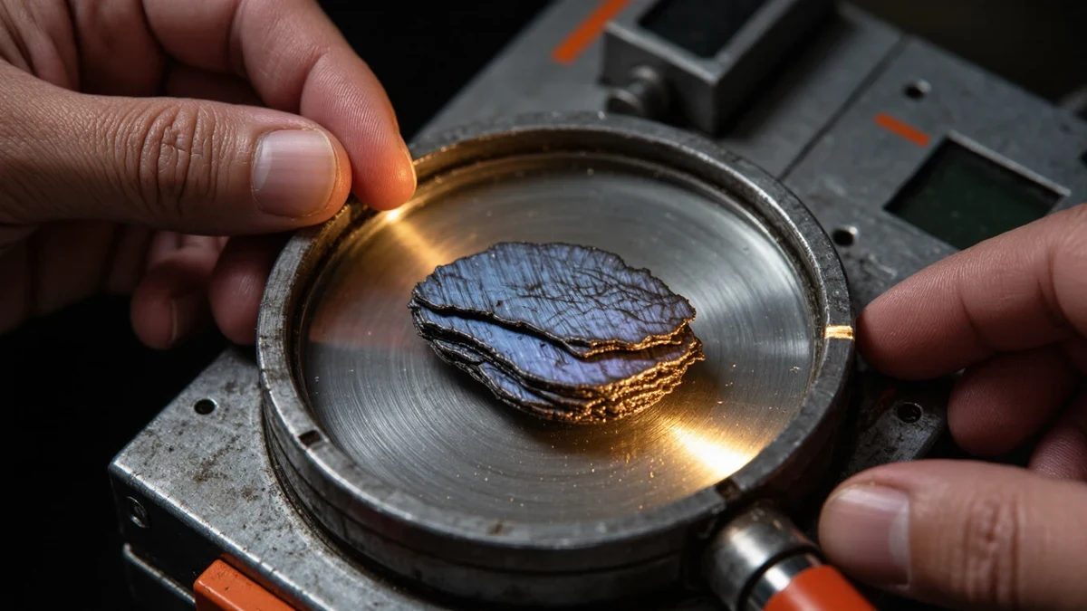
Supply concentration added a second layer of difficulty. Production methods range from tape exfoliation, fine for laboratories, through chemical routes to the methane-decomposition processes used for commodity volumes. Each yields different material at different cost, and claims of tonnage capacity have historically outpaced verified deliveries — which is why the Tabuk figure carries its company-claimed label here, and why buyers in this industry habitually ask for certificates of analysis rather than datasheets.
Who is actually building the factories?
The 2025 picture, per the Guardian's survey of the UK scene, is one of narrow but real industrial bets. 2D Photonics, working on graphene photonic chips, has raised 25 million pounds and plans a pilot manufacturing site in the Milan area to produce 200mm-wide wafers at scale. Paragraf, a sensor maker, has raised 55 million dollars. Graphene Innovations Manchester, working on graphene-enriched carbon fiber, has begun production in Tabuk with a local partner and says it is on track to produce 3,000 tonnes by 2026 (company-claimed).
Three different products, three different processes — which is precisely the point. The graphene industry stopped seeking a single killer application and started shipping application-specific material: sensors on wafers, additives by the tonne. That fragmentation reads as weakness in a market report and functions as strength on a factory floor.
What did the latest research actually show?
On the research frontier, the headline result of late 2025 came from Monash University's reported results, whose team found graphene-based supercapacitors with record volumetric performance. In pouch-cell devices built from a material the researchers call multiscale reduced graphene oxide, the devices reached up to 99.5 watt-hours per liter and power densities as high as 69.2 kilowatts per liter, with the team describing the metrics as among the best ever reported for carbon-based supercapacitors (published in Nature Communications, December 2025). The mechanism, per the researchers: changing how the material is heat-treated unlocks far more of its internal surface area.
Energy storage is the application where graphene's surface-area economics align best with a real market — fast charging, long cycle life, transport electrification. Supercapacitors are a niche today; the significance of the Monash result is the manufacturing angle, since the team emphasized that the process is designed for scalable production rather than bespoke lab conditions.
What should engineers and buyers watch from here?
A skeptic's checklist for any graphene claim, in order of usefulness:
- Which graphene? Flake, oxide, film and wafer are different materials with different costs; unnamed graphene is a marketing word.
- Tonnage and price, not capacity claims. The Tabuk plant's 3,000-tonne target is a company-claimed milestone — watch for independent confirmation and per-kilo pricing.
- Certified consistency. The graveyard companies failed on batch-to-batch uniformity, not performance peaks.
- One application per supplier. The survivors — sensors, photonics, additives — each sell one thing that works, and that restraint is the signal.
Twenty years in, graphene has stopped being a promise about everything and started being a set of specific products with specific numbers attached. That is what a real advanced material looks like right before it gets boring — and boring, in manufacturing, is the goal.